
 I first read about the Mini-Circuits PMA5-123 3W GaAs MMIC device on the UK-Microwave forum early this year. Thanks to the efforts of Kent – WA5VJB, Maarten – PA0MHE and Rens -PA3AXA (and possibly others I’m not aware of) several of us came away from the Martlesham Microwave Round table with one or more PA kits comprising of a PMA5-123 device and PCB.
Like possibly many others I was surprised just how small this 3W rated chip was and immediately wondered how I was going to solder it in place. If you don’t already know, it’s a 5 x 5 mm 32 lead QFN style package, a small, thin, leadless package with electrical contacts on the bottom surface.
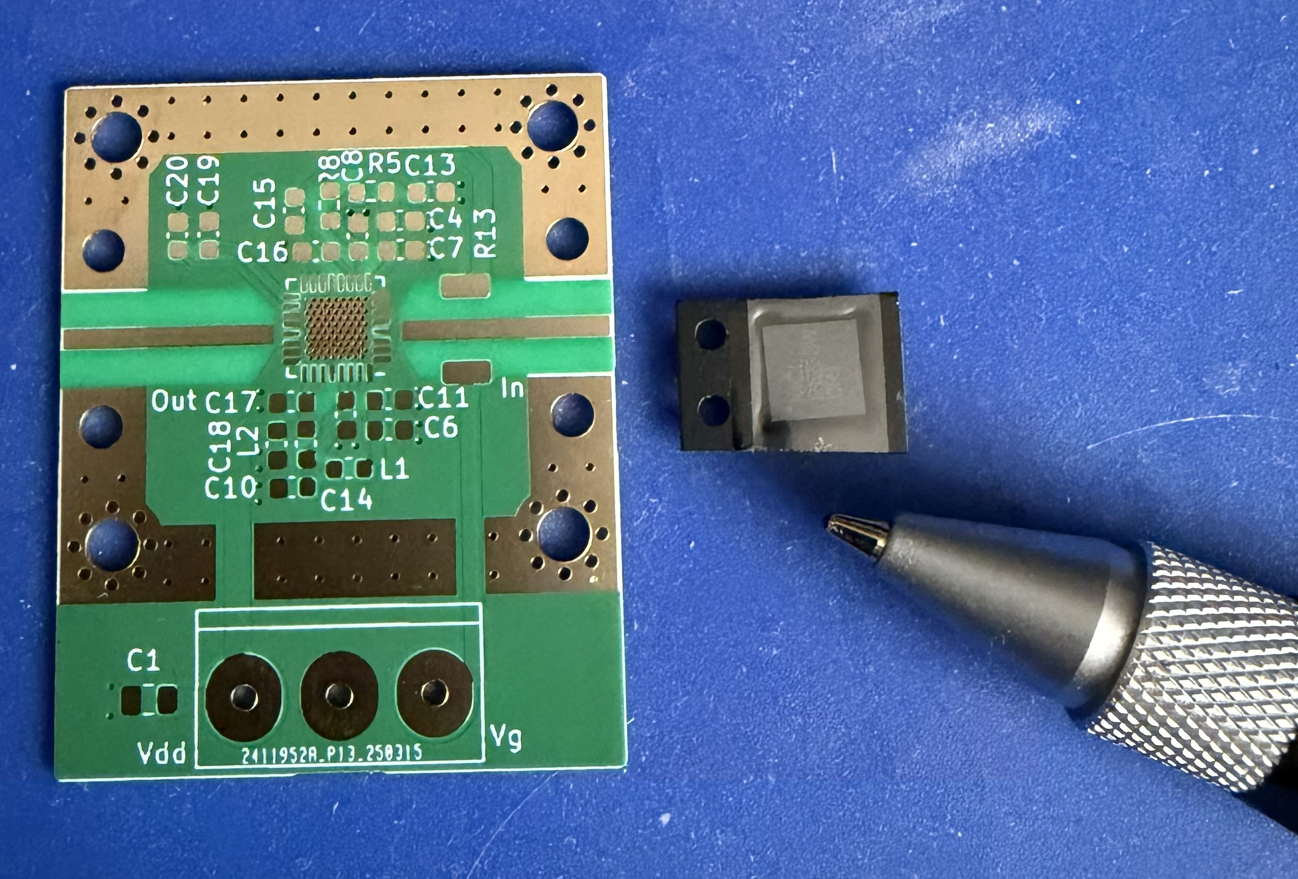
PMA5-123 Chip with Ball Pen For Size Comparison
Having no experience of working with such devices I (and maybe many others by all accounts) decided to wait and see how others got on soldering them in place and what sort of power out they were able to achieve. To date there appears to be very little information online detailing output power, successful / unsuccessful builds, other than what I’ve seen here.
During a QSO on QO-100 with Chris – G8BKE we established that we had each got these kits and were both wanting to get on and build a working PA. Following an exchange of emails where I learnt some tips on how to hand solder the PA device I placed an order for a small number of DC-bias boards and we both started to gather the additional parts needed.
The DC-Bias board ensures that the PA state is managed correctly when powering on / off and between RX/TX. It also has a calibration routine to set a defined Iq and maximum Id value. All this is controlled by an onboard ATtiny412 MCU. Fortunately the control software was also made available, but how to program the ATtiny412 was another unknown to me.
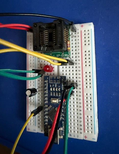
While waiting for all the parts to be delivered I read up on how to program an ATtiny chip using an Arduino Nano as a UPDI programmer. Several different articles described how to do this, all with varying amounts of detail, I chose to follow one by Electronics-Lab. I wanted to be able to upload the program to the ATtiny before soldering it in place. A special adapter (SOP8/16 to DIP8/16 socket) was purchased to be able to physically connect the ATtiny chip to the breadboard based Arduino UPDI programmer. To prove that things were working, an LED and resistor were also added so that a simple “Blink Sketch” could be uploaded to check that everything was working and the LED did blink.
With the exception of the DC-DC chip that’s used to provide the negative Gate volts I then soldered both the PA and DC-Bias boards by hand. As all the contact pads are on the underside of the DC-DC chip I needed to use a hot air gun to mount that component. For this reason the DC-DC chip was the first component to be soldered in place. A small number of SM components were then added to be able to test that the chip had soldered successfully and the Gate supply was working correctly.
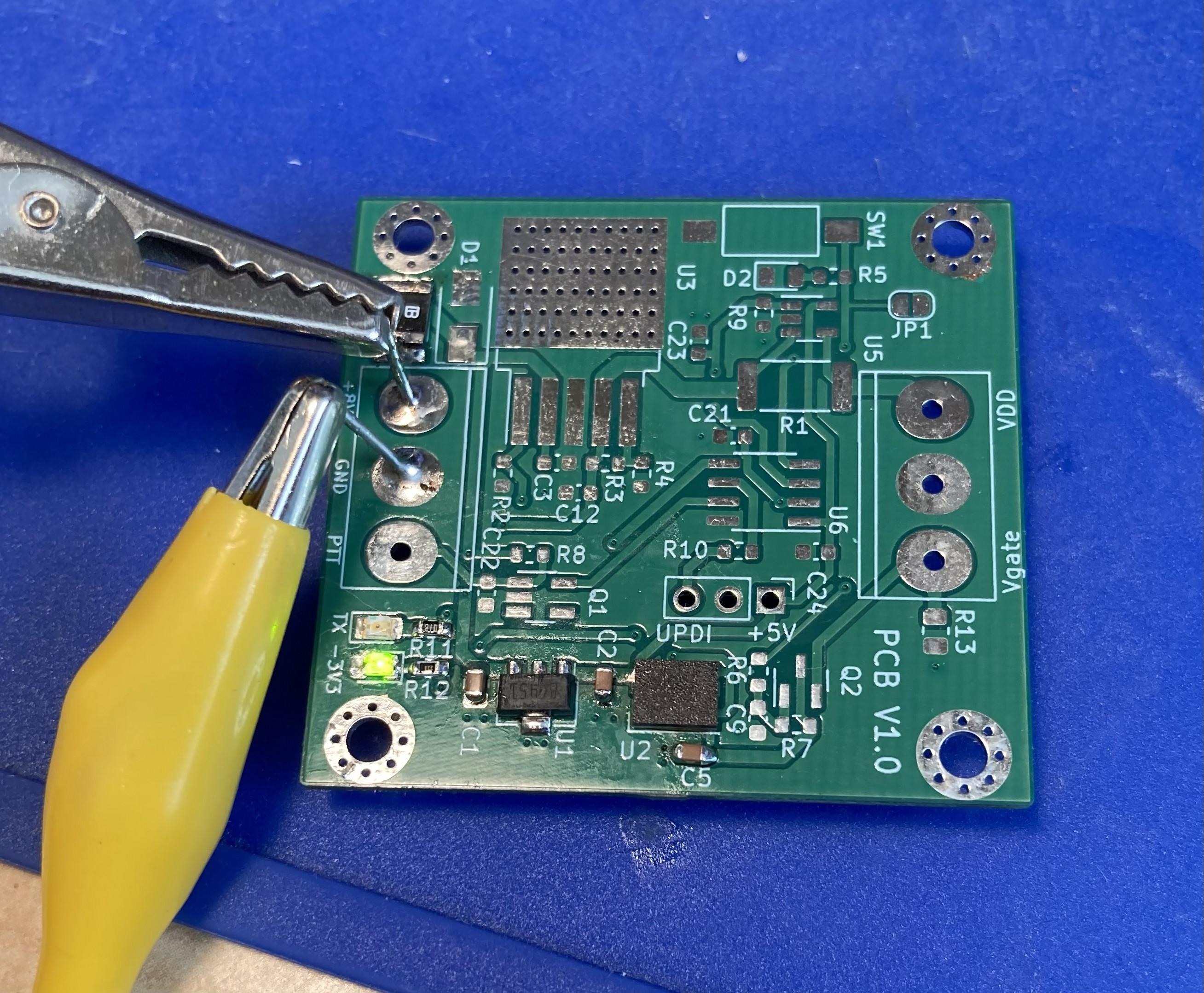
Photo showing DC-DC negative Gate volts supply being tested as first stage of build and before any board cleaning!
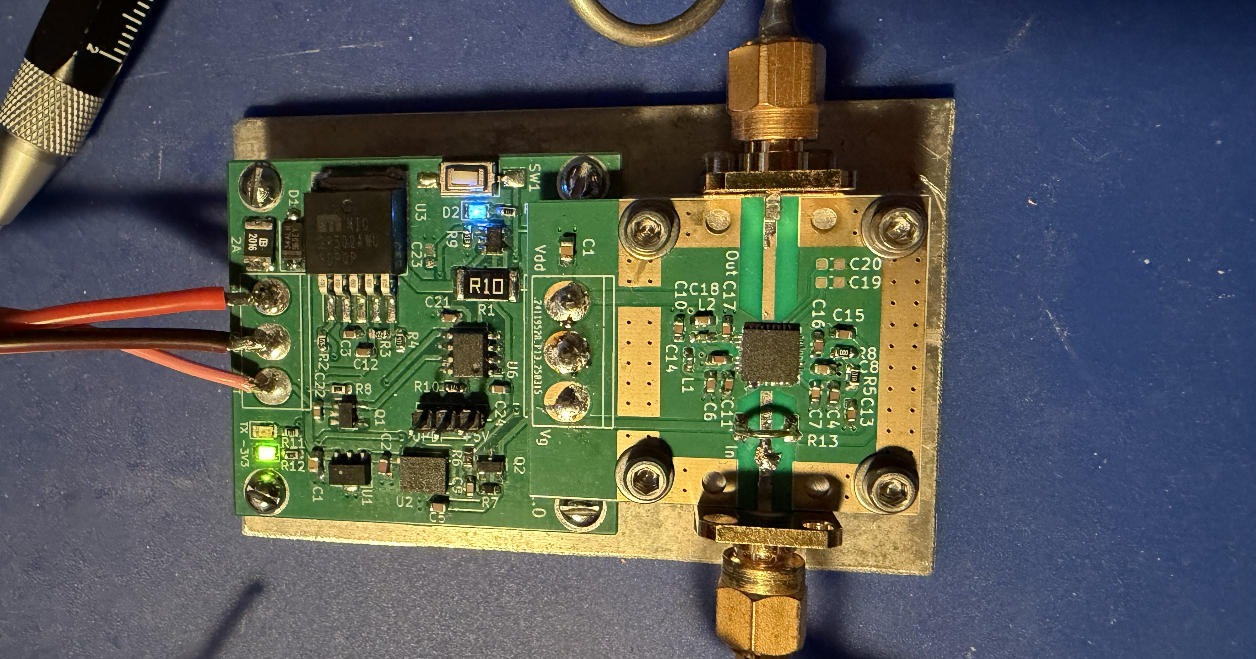
Both boards use QFN devices and the majority of other parts are 0603 sized which proved to be right on the edge of my hand soldering capabilities nowadays. But with patience, a good iron and lots of flux both boards went together without too much grief. The DC-Bias board was tested to ensure that the negative Gate voltage was present at all times and Drain volts were correct when the PTT line was grounded. A large fixed resistor was also used as a temporary load to “stress test” the Drain supply to 1A.
Once the basic checks were completed the DC-Bias board was connected to the PA, 2 SMA 50R dummy loads were put on the input and output of PA. With a current meter in the power lead and 9V applied the meter showed approximately 50mA. At this point the Blue LED was flashing to indicate that the calibration had not been done. The 9v supply was disconnected, the calibration button on the DC-Bias board held down and the 9V reapplied. This initiated the calibration routine, the TX LED came on until the calibration was completed and the memory updated. Once this had been done the PTT was grounded and the meter showed the expected 450mA. This was a very pleasant surprise as I should confess to having to remove and resolder the PA chip as I somehow managed to mount the thing 90 degrees out the first time! Fortunately I noticed this after I cleaned the board with IPA and before any volts got near it.
What followed next was a series of tests and measurements with various drive levels between 0 to +14dBm. For this I used my test source plus a “Franco” amplifier board with various fixed attenuators. Power measurement was done using an HP432A + sensor.
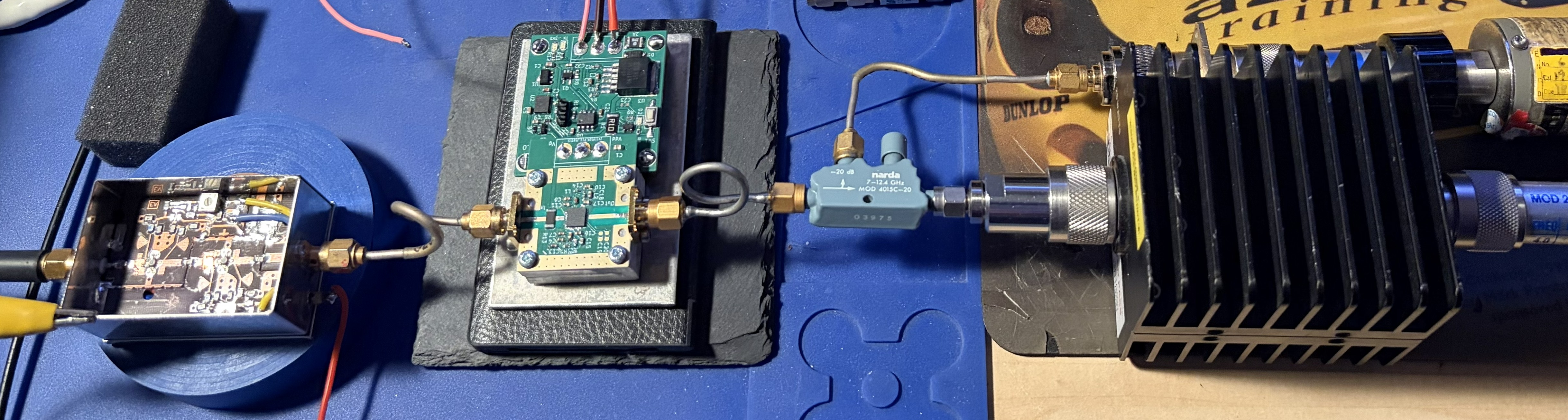
Initial test setup. PA heatsink 30x28x12.5mm Ali block.
With the Iq set to the programmed default 400mA and IdMax at 1.25A I struggled to get more than 1.1W out and the gain was way below an expected value of around 26dB. I then experimented with different Iq settings and reached a point where I was seeing almost 2W out. Increasing the drive would cause the Drain current to exceed IdMax (1.25A) and the DC-Bias board would trip to fault mode.
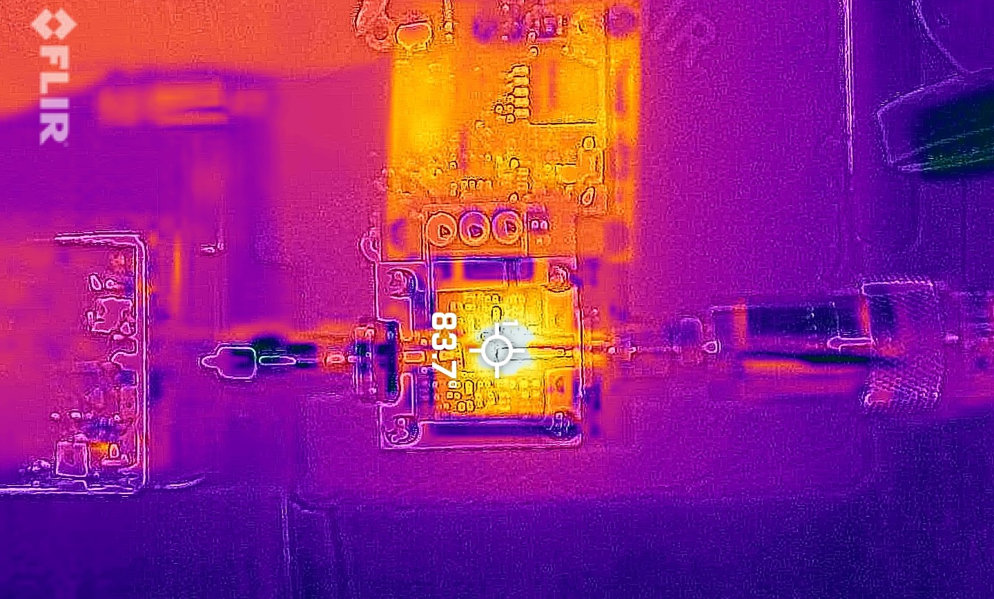
A very quick look at temperatures. 1.5W out.
After an exchange of ideas via email, a number of small changes to the PA board and ATTiny SW were made which resulted in significant improvements. The PA is now producing 2 – 2.5W with 24dB gain which is ideal for it’s intended use as a PA for my modular 10GHz TVTR.
The following changes were made:
- R13 0R chip resistor was replaced by an elevated wire bridge. This improved the impedance / match and resulted in almost 2dB extra gain.
- A small snowflake (piece of copper foil) was added to the input track which improved the impedance / match resulting in a small increase in gain.
- The Iq value in the software was changed to allow Iq=500mA
- The IdMax value in the software was changed to allow Id maximum of 1.5A
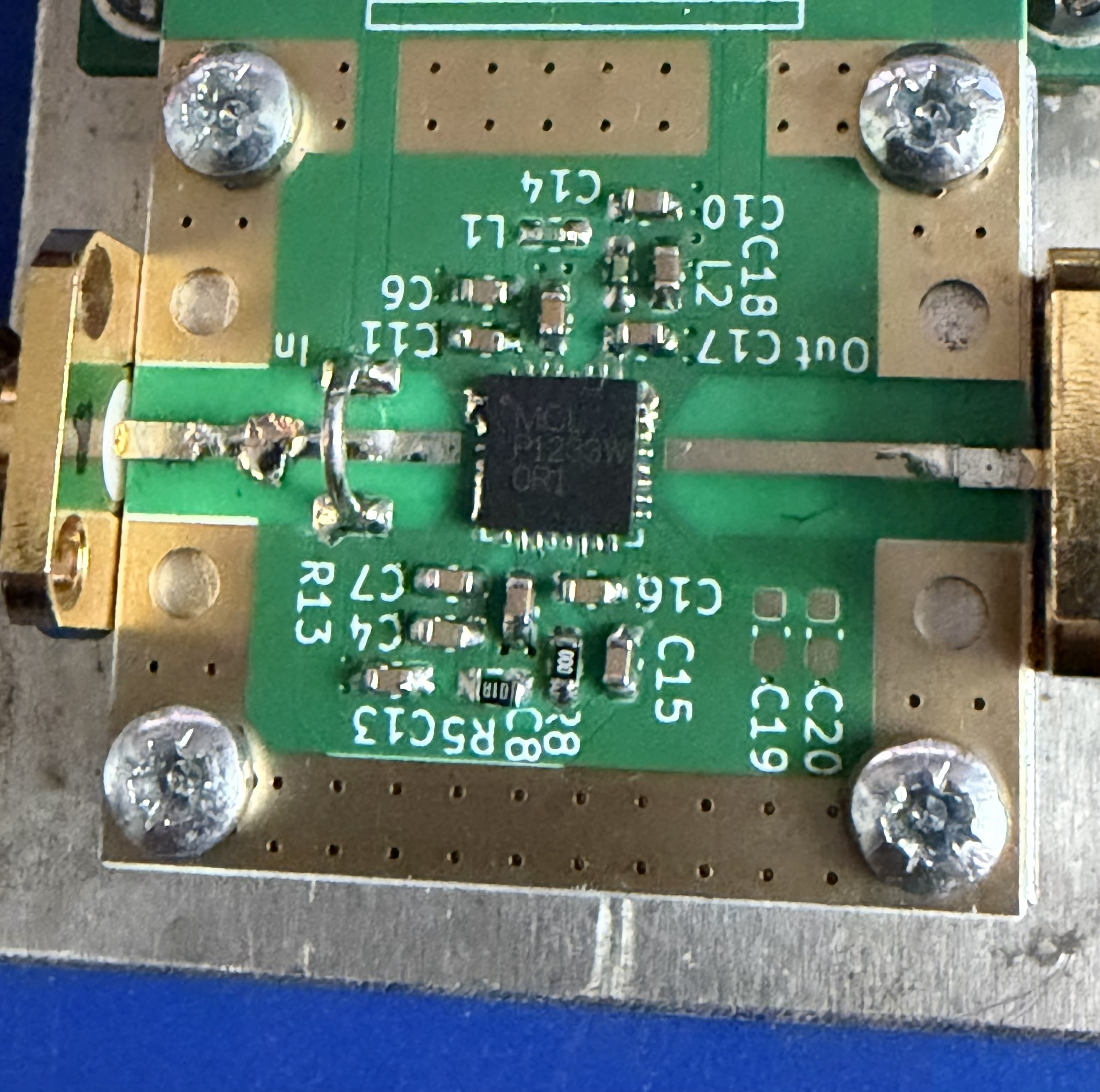
Photo showing snowflaking and wire bridge modifications
The results so far are very encouraging, with an output of typically 1 to 2W it should make a nice PA for many of the transverters that are in use today. Will it give more output, I’m sure it would, but for how long?? It’s a very small chip with an equally small surface area that’s in contact with the heatsink, so cooling is a challenge.
What’s next?
- The PA needs some form of enclosure, I’m currently exploring two possible solutions, one just for the PA board and another that houses both boards.
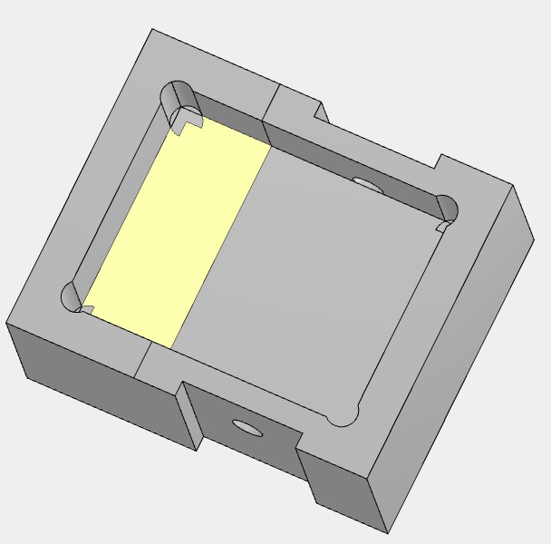
Option 1 PA Only, 50x40x22mm with 12mm thick floor for heatsink
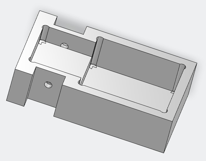
Option 2: PA and DC-Bias boards. 85x50x22mm with 12mm heatsink section under the PA board.
- Do further tests / measurements both RF and temperature once the PA is fitted into an enclosure.
- Add this to my modular 10GHz TVTR and shoehorn everything into the waterproof housing that has sat gathering dust for far too long.
- Build an Arduino controlled hot-plate to (in theory) make the soldering of QFN devices so much easier.
- Build the second pair of boards that I have sat here destined for my /P TVTR.
- Update: See here.
Acknowledgements:
- Thanks to Kent – WA5VJB, Maarten – PA0MHE and Rens -PA3AXA (and possibly others I’m not aware of) for their part in this project. All the information needed, i.e. BOMs, Gerbers, ATtiny SW etc can be found here.
- Chris – G8BKE for sharing this build experience with me.
- Gus – G3ZEZ for producing the heatsinks.
